Monday, December 8, 2014

ERIC-1: Video Memory Interface

The ATmega1284P coprocessor of ERIC-1 has been able to output a PAL video signal for some time. As you may know, the coprocessor has a screen buffer of 50x32 characters and a 2KB character rom table storing the glyphs of the character set. All this data is stored in ATmega's internal SRAM and so far there has been no communication between the 6502 and the coprocessor. Thus the contents of the screen has been fixed.

Recently I have been working on getting the 6502 talk with the coprocessor, so that a region in 6502's address space is mapped to characters on the screen. In this blog post I'll review some alternative ideas that I considered before settling on the final design.

Time is of the essence


The ATmega has 16 kilobytes of internal SRAM memory which is really fast (it can read or write a byte in 2 cycles), but there is no way to read data fast enough from an external memory chip during PAL video generation. Therefore, the only possibility is transfer the needed bytes from the external SRAM chip to the internal SRAM during the scanlines when the ATmega is not outputting pixels. The screen mode I'm using has 256 lines of vertical resolution and a progressive PAL frame has a total of 312 lines, so luckily I have plenty of free scanlines to do the memory transfer. I figured the best time to do it is during the top border area, that is made of 32 blank scanlines before the visible image starts.

But it's not that simple. The ATmega can't just go and peek and poke to the memory anytime because the 6502 is executing and accessing the memory all the time. There are at least three ways to solve this problem. Firstly there are dual port memory chips that can deal with memory accesses from two sources at the same time. This kind of memory is more expensive and was not used in the 80s microcomputers. I felt that this design would not be in the spirit of the 80s micros and besides I already have my regular 628128 128K x 8 SRAM chip plugged in, so I dropped this idea.

The VIC-20 and C64 solved this problem cleverly by timesharing. The internal architecture of the 6502 is not pipelined and it can only access memory when its clock signal is high. The VIC-I and VIC-II graphics chips in VIC-20 and C64 take advantage of this and access the memory when the clock signal is low. This is a really neat because both chips can think that they own the memory all the time. The disadvantage of this approach is that the video chip and the 6502 are executing in lockstep. Basically the clock frequency of the 6502 of these systems is fixed to about 1 MHz and trying to change this will mess up the video chip timing badly. I considered implementing this idea and I think it could very well work. Since the ATmega is generating the clock signal, it knows in which state the 6502 clock is. Clocking the ATmega at 16 Mhz and 6502 at 1 MHz, the ATmega would have 16 cycles for every 6502 clock cycle. This could be just enough time to access the memory. Maybe something along the lines of this pseudo assembly routine could do the trick:

I haven't tried this approach yet, because it would be pretty much impossible to verify the timing without a logic analyzer or oscilloscope. Without exactly correct timing bad things will certainly happen.

But there is a third, much simpler way and this is what I ended up doing. The ATmega is generating the clock signal and it can halt the 6502 whenever it needs to access the memory. Now that I have upgraded the CPU, halting it is ridicuously simple. I just have to set the ATmega timer frequency to zero and the clock will stop in whatever state it was. Resuming the clock is as simple, I can just reset the timer frequency to whatever value it was. This solution has the nice property that the 6502 can be clocked independently from the video chip so 4 MHz system clock or even higher is no problem at all.

Here is the piece of code I'm using to halt and restart the CPU:

Block transfers


The memory transfers are implemented in the firmware in copymem128 routine. The routine halts the CPU, copies a 128 byte block from external SRAM to internal SRAM of the ATmega and resumes the CPU. The routine is called by the first 13 scanlines just after the vertical sync. In total 13*128 = 1664 bytes are copied, which is a few bytes larger than the screen ram. The screen ram used to contain pointers to character data, but I have changed the screen ram to contain character indices instead. This cuts the number of bytes to be copied over to half.

All the bytes copied are always on the same 256-byte page of RAM, so only the low byte of the address needs to be updated during the memory copy.

Here is the piece of code that copies the 128 bytes. I had to insert an extra nop in the loop, otherwise the data would not be copied correctly. Even without the nop, the latency should be within the specs of the 70ns SRAM, so I suspect that the breadboard must be caused problems here. I will try to optimize the nop away when I will eventually build this on the PCB.

Why 128 bytes? I would have hoped to copy an entire 256 byte page per scanline but unfortunately there is not enough time per scanline to copy an entire page. The ATmega has only 1024 cycles per scanline.

Test program


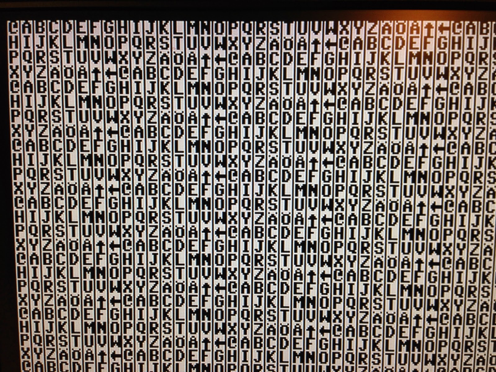
Finally the project is in a state where the 6502 can do something visible. To test the video memory interface I assembled a small 6502 program to update bytes in the screen memory area. It first clears the screen and then prints some text on the screen in a loop. Printing has been artificially slowed down by adding a delay loop because a 6502 running at 1 MHz is such a beast ;-).

Below is a video showing the output of the test program and the 6502 source code. Writing larger programs is going to be really tedious by manually typing in opcodes, I need to get a real assembler soon!

Thanks for reading! As always you can find the latest version of the source code at GitHub.


Sunday, December 7, 2014

ERIC-1: CPU Upgrade

I recently got a delivery of two brand new W65C02S chips from Coltek UK (£9 for two chips including shipping to Finland, not bad!). Now, if this didn't ring a bell, here's some news for you: 6502 microprocessors are still made even today. According to Western Digital Center (WDC), the owners of the 6502 intellectual property, hundreds of millions of 6502s are still made each year. Applications listed on their website includes scanners, toys, dashboards, industrial controllers and all sort of other embedded device, the list is long. Not bad for a CPU made over 30 years ago!

The processor chips I received are from these newer generations of 6502s made by WDC and they have some major improvements over the old Rockwell 6502 I had obtained earlier. First, the W65C02S version has a fully static design, meaning that it no longer loses the state of its internal registers if the clock is stopped. This makes single-stepping and halting the CPU much easier. I no longer have to wait for the clock and R/W to be high when stopping the CPU. Nice!

Also there is a new pin, the bus enable BE pin. When it is low, the address, data and R/W pins go to high impedance state (meaning they are essentially disconnected). This is a really handy feature that can be taken straight away into good use in ERIC-1. The W65C02S can also support clock frequencies up to 14 MHz (max for a Rockwell 6502 is 4 MHz). The breadboarded ERIC-1 probably can't sustain clock frequencies that high due to stray capacitance effects and long wires of the breadboard, but it's good to have that option when I will eventually build this on a PCB. WDC also has implemented a few new opcodes but I haven't taken a closer look at them yet.

The W65C02S is almost a direct replacement for the R65C02 but there are a few important details. The RDY pin is now bidirectional when it used to be only an input pin. There's a new instruction WAI that puts the RDY pin into output mode. Therefore it's important that this pin is not pulled up by connecting it directly to VCC or you could risk causing a short if the pin goes to output state. Instead a pull up resistor needs to be used. Well, I was already doing that so no problem. Another gotcha is the new function of pin 1, which used to be GND on Rockwell but it's now an output pin. According to the datasheet pin 1 is now labeled Vector Pull (VPB) which indicates that a vector location is being addressed during an interrupt sequence. I don't know what it is used for but better leave that unconnected.

With the new BE pin I was hoping to get rid of the 74HC541 buffers that I was using the detach the 6502 from the address bus when the coprocessor needs to access memory. I replaced the old Rockwell with a W65C02S and replaced the buffer chips with jumper wires. I also needed to invert the sense of the BE signal in the ATmega firmware: 74HC541 have OE which is active low, where as BE is active high on the W65C02S. I made the changes and everything seemed to work correctly.

After some time however I noticed a problem. The ATmega refused to be reprogrammed. I'm using an USBTiny programmer to update the ATmega firmware and it is connected to the SPI pins of the ATmega. The same pins are also mapped to I/O port B which is connected to the address bus on the 6502, so I suspected that there must be bus contention going on when the programmer is attempting to reprogram the chip but the 6502 is still driving the same lines for some reason. I disconnected the address lines on the SPI pins and sure the problem went away. This was really strange because the same setup used to work with the 74HC541 buffers. The W65C02S bus drivers must be somehow different than the 74HC4541 buffers or I must have made an error somewhere. It could be some sort of timing issue. According to datasheets the propagation delay for a '541 is typically 10ns and W65C02S BE was max delay of 30ns. Is this enough to make a difference? I doubt it. Anyway, I haven't yet been able to solve this mystery yet.

Even with the internal bus drivers of the WDC chip, one 74HC541 must remain for buffering the CE signal for the SRAM chip (when the ATmega accesses memory it needs to take over the SRAM CE signal and the simplest way to do this is to detach the CE from 6502 using a '541). As a workaround for the reprogramming issue, I routed three address lines through the same 74HC541 that is used to buffer the CE signal.

With these changes the WDC 6502 can now coexists happily with the ATmega1284P. With two chips gone the design now simpler but I'm still not entirely happy with the results. The strange issue with the firmware updates is still an unsolved mystery and routing the three address lines through the buffer feels like a kludge fix. The kind and wise folks of the 6502.org forum have given me some ideas to try to solve this mystery. I've also ordered a Saleae logic analyzer which should come in handy in debugging these kind of problems. I'll probably revisit this issue later armed with proper tools.

The new upgraded ERIC-1 with a W65C02S. Two 74HC541 chips from
the earlier design have been removed.

Updated schematic. The remaining 74HC541 has a dual duty: it takes care
of buffering the SRAM CE signal and also disconnects the three address
 lines A12-A14 when ATmega's firmware is updated.

Wednesday, December 3, 2014

ERIC-1: Bitbanging the video signal

I've been working on video signal generation for my ERIC-1 microcomputer lately. As you may know I built a 8-bit console in the past that generated a composite video signal using an ATmega328P microcontroller. The microcontroller outputted an 8-bit color value every 5th cycle which resulted in a pretty low resolution image. A DAC resistor network and a AD725 chip was used for RGB to PAL color conversion. For ERIC-1 I'm taking a bit different route, mainly because I want to get at least 40 characters per line on the screen and this requires higher resolutions than was possible in the console project.

Life and deeds of PAL video signal


A progressive PAL video signal is actually quite simple. A single PAL frame has 312 lines and the lines have the following structure. The first 5 lines indicate the start of a new frame and they provide the necessary vertical sync signals for the monitor to sync to. After that the next 304 lines contains the visible image, although some lines, typically the first 20 lines at the top and last 20 lines at the bottom, are clipped off by the monitor. The exact number of clipped lines depend on the monitor or TV. Finally after the visible image comes 3 lines that again contain vertical sync signals and tell the monitor to jump back to the top of the display.

Each PAL scanline is exactly 64us long. The sync lines are made of a series of long and short pulses. A long pulse is 30us low followed by 2us high state. A short pulse is 2us low followed by 30us high state. These pulses are used to generate the sync signals as follows:

Line
1 Long Pulse Long Pulse
2 Long Pulse Long Pulse
3 Long Pulse Short Pulse
4 Short Pulse Short Pulse
5 Short Pulse Short Pulse
6-309 Visible lines
310 Short Pulse Short Pulse
311 Short Pulse Short Pulse
312 Short Pulse Short Pulse

Every visible line starts with a horizontal sync pulse for the monitor. The HSYNC is 0V for 4.7us. The HSYNC is followed by a "back porch", which is 0.3V for 1.65us. In case of a color signal, a special color burst signal is generated during the back porch, but since we are at the moment dealing only with black and white images, we can skip this detail. After the back porch the remainder of the scanline contains luminosity data in range 0.3V (black) to 1V (white).

Since I'm using a ATmega1284P microcontroller which can only output digital values that are either 0V (low) and 5V (high), how can I generate the needed voltages? For black and white image, the needed voltages are 0V (HSYNC), 0.3V (black) and 1V (white). The crucial point to understand is that there is essentially a 75 ohm resistor inside the monitor which terminates the composite video signal to ground. This is called the input impedance and the value of 75 ohms is determined by the PAL standard. With this information it's simple to come up with the following circuit:

SYNC, VIDEO and GND coming from left, monitor on the right.

The 1K resistor and the 75 ohm "resistor" inside the monitor form a voltage divider. When the SYNC signal is high, the monitor receives the following voltage: 75 / (1000 + 75) * 5V = 0.35V. Similarly the 470 ohm and 75 ohm resistor form another voltage divider that sets the voltage level at the monitor input to 75 / (470 + 75) * 5V = 0.7V when the VIDEO signal is high. With different combinations of SYNC and VIDEO values we can generate the voltages 0V, 0.35V and 1.05V. Close enough to what we need!

The lost art of cycle counting


So, to generate a PAL frame we need to change the values of the two output pins SYNC and VIDEO very fast. These signals will get converted to proper voltage values by the two resistors. But how fast exactly do we need to change the pins, or "bitbang" them? Well, quite fast for a microcontroller running at 16 Mhz... A single scan line is 64us long and a MCU running at 16MHz has 16 clock cycles per microsecond. Therefore during a PAL scanline we have 64*16 = 1024 cycles. In 1024 cycles we have to generate the HSYNC pulse, the back porch pulse and the visible pixels. That means there's only time for a couple of clock cycles per pixel!

In the console project, I used a timer interrupt to trigger a routine every 64 microseconds. But interrupts have a rather large overhead on the time scale we are working with here: registers have to be restored and jumping to and back from the interrupt routine takes time. This time I decided to do this more efficiently. I have written the video signal generation entirely in assembly and explicitly cycle counted the code so that each scanline takes exactly 1024 cycles to execute. After a scanline has been processed I can immediately begin generating the next scanline. A very nice thing with this approach is that I can keep important values such as line counters and memory pointers in registers all the time.

Every scanline begins with the HSYNC signal, which is 4.7us in length. At 16Mhz that is 75.2 cycles, so we round to 75 cycles. Then the back porch is 1.65us and rounded to cycles it becomes 26 cycles. In assembly we can cycle count and output the HSYNC and back porch in 75+26  cycles. Then we have exacly 1024-75-26 = 923 cycles left for the pixels. Let's round this to 900 cycles because we need some cycles for housekeeping stuff like incrementing the current line counter and jumping to the routine processing the next scanline. For e.g. 320 pixel horizontal resolution that would be only 900/320 = 2.8 cycles per pixel. Pulling a pixel from MCU's internal SRAM takes 2 cycles and outputting a pixel takes 1 cycle so at minimum we would need at least three cycles even when doing simple direct bitmapped graphics. Initially it seems there is no way get what we want with this microcontroller.

To make matters worse, a bitmapped image takes a lot of memory to store and is very heavy for the 6502 to process. That's why 6502 computers usually have a character based display mode, where the screen RAM contains indices or pointers to character data stored elsewhere in memory. For example, the screen of a C64 is divided into 40x25 characters and each character is 8x8 pixels. So for every 8th pixel the video generator has to fetch the character from screen RAM and then pixels from character memory. All this increases the cycle cost way higher than 3 cycles per pixel.

Attempt that almost worked


Luckily there is a faster way to get bits out of the ATmega1284P. The ATmega1284P has a built-in Serial Peripheral Interface (SPI) which is essentially a shift register whose clock frequency can be configured. The maximum rate for SPI is system clock divided by two, that is 8 MHz in our case. After the SPI has been initialized, a byte can be outputted by writing it to the SPI data register. The SPI hardware then shifts outs the bits at 8 Mhz, i.e. at 2 cycles per pixel. What's great is that the SPI runs independently so we can execute other instructions while the SPI is doing the transfer. Ok, I wired this up and wrote a scanline routine that pull a character from memory, fetches a byte encoding the 8 pixels of a character line and outputs the byte using SPI.

Initial results were very promising. I could get 320x256 resolution and even higher seemed possible. However, then I hit a major snag! See image below.

Argh, those black vertical gaps between characters!

These is a one pixel gap between every character. Even when I waited for exactly the right number of cycles, I got this gap or either corruption on the screen. I was pretty sure I was doing everything right and it felt like a hardware problem. Googling revealed a nightmare: this is a known hardware limitation, the SPI cannot send a continuous stream of bytes, apparently because there is no buffering. There is just a single register that gets shifted out and the hardware needs one extra cycle to load the shift register between transmits.

This was such a major setback. It seemed I would have to live with the gaps. This didn't seem like a good idea because I want to get nice character based graphics out of this thing eventually and having gaps there would certainly ruin it in a major way.

USART MSPI to the rescue!


I thought about using an external shift register as a workaround. A byte would be loaded one at a time using 8 parallel I/O pins (+ some control pins for clock signal et.), but I was already very tight on I/O pins so I couldn't afford this. I was really frustrated and considered even abandoning the idea of bitbanging the video signal using a MCU. But then after reading the datasheets carefully I learned there was another way: the built-in USART which could send data through the SPI, called the "USART in MSPI mode". The USART has a transmit buffer, so maybe the hardware could be the magic I needed to fix the gaps? A quick Googling seemed to indicate that this could be possible. So last night I make the necessary changes and nervously fired up my microcomputer... and huzzah, the gaps were gone!

With this victory under my belt, I optimized the code further. I could now output a 8 pixel wide character in just 16 cycles, including the screen RAM to character data indirection. With this I could extend lines to 50 characters, yielding a resolution of 400x256. The character generation now needs 50*16 = 800 cycles so there is still some time left. I could still extend the screen width a bit, but I'm going to settle for this nice round number for now.

You can find the source code of the project at GitHub. The screen contents is so far stored in ATmega's internal SRAM and completely static. Next I'm going to interface it with the 6502 and then the real fun can begin!

Finally here's a final gapless screenshot using a very familiar character set.